
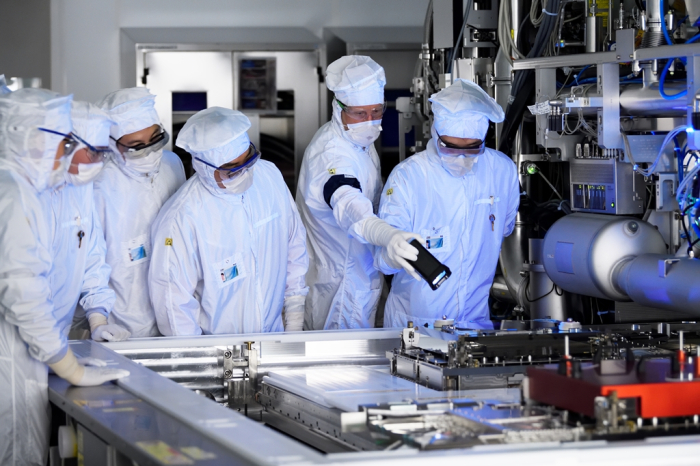
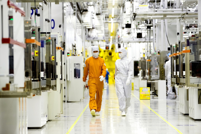
Samsung Electronics Co., a leading memory chipmaker, is making a renewed bet on next-generation semiconductor manufacturing, committing 1.1 trillion won ($773 million) to acquire two of ASML Holding N.V.’s most advanced extreme ultraviolet (EUV) lithography machines by mid-next year – a move seen as a critical step to regaining its technological edge in the global chip race.
According to industry sources on Wednesday, the South Korean tech giant is expected to take delivery of its first high-numerical-aperture (high NA) EUV scanner, the Twinscan EXE:5200B, later this year, followed by a second unit in the first half of 2026.
While Samsung already operates a research-use high NA EUV tool at its Hwaseong campus, the upcoming machines mark its first purchases intended for mass production, sources said.
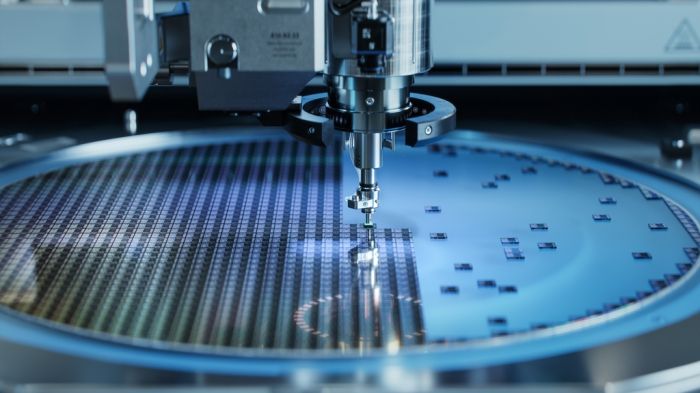
The high NA EUV system, developed by ASML, the world’s only maker of EUV lithography machines, can etch circuits 1.7 times finer than those produced with current-generation EUV tools.
The key improvement lies in the system’s numerical aperture – a measure of how effectively the lens gathers light – which has been raised to 0.55 from 0.33.
Each unit costs roughly 550 billion won, making it the most expensive piece of equipment in semiconductor manufacturing, according to industry officials.
“Samsung is placing a major bet to push the boundaries of next-generation process technology,” said an industry executive.
CHAIRMAN LEE’S PERSONAL INTEREST IN HIGH NA EUV
Samsung Chairman Lee Jae-yong’s interest in high NA EUV began in December 2023 when he visited ASML’s headquarters in the Netherlands.
Impressed by its potential to enable chip production below the 2-nanometer threshold, Lee reportedly instructed engineers to accelerate development of compatible process technologies.
Samsung’s decision to introduce the latest tool for volume production suggests that its process engineers have now reached that point, sources said.
Rival foundries, or contract chipmakers, such as Taiwan Semiconductor Manufacturing Co. (TSMC) and Intel Corp., are testing R&D versions of the system but have yet to adopt them for commercial-scale manufacturing.
Apart from Samsung, SK Hynix Inc. is the only other chipmaker known to have ordered a production-grade high NA EUV unit, announced in September, sources said.
FOUNDATION FOR AI-ERA SEMICONDUCTORS
Samsung was the first in the industry to apply conventional EUV lithography to its 7 nm foundry line in 2018 and later to DRAM production in 2020.
The new high NA generation represents the next leap, enabling ultra-precise patterning required for advanced chips that power artificial intelligence and data-intensive applications.
Sources said Samsung plans to deploy the new machines at its 2 nm foundry lines, which already produce Exynos 2600 application processors.
The Korean chipmaker also plans to make and supply Tesla Inc.’s next-generation AI chips at the 2 nm foundry lines using the latest EUV equipment, they said.
The tool will also underpin production of Samsung’s future vertical channel transistor (VCT) DRAM, high-performance, low-power memory chips slated for mass production around 2027.
Analysts said the move signals that Samsung, after a period of cautious capital spending, is shifting back into aggressive investment mode to close the gap with competitors, including dominant foundry player TSMC.
Samsung has recently narrowed the performance divide with SK Hynix in next-generation high-bandwidth memory (HBM), unveiling plans this week in San Jose to push data rates for its upcoming HBM4E chips to 13 gigabits per second per pin – faster than current industry offerings.
As one Seoul-based semiconductor analyst put it: “Samsung’s early adoption of high NA EUV could be the catalyst it needs to reassert leadership in both logic and memory at a time when AI computing is reshaping the entire chip landscape.”
By Jeong-Soo Hwang, Chae-Yeon Kim and Eui-Myung Park
hjs@hankyung.com
In-Soo Nam edited this article.