 |
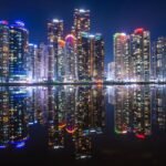
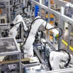
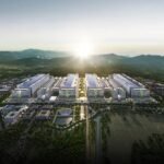
Debate over Samsung, SK Hynix’s second chip cluster in Korea heats up: Is it feasible? The Honam region in southwestern S. Korea offers ample land, water, and power for the planned chip cluster, but faces steep hurdles in attracting top-tier engineering talent and supply chain vendors ByChae-Yeon Kim, Hae-Ryeong Kang and Kwang-Sik Lee / Published: June 28, 2026 at 9:00 AM(KST) South Korea, home to Samsung Electronics Co. and SK Hynix Inc., is locked in a heated debate over plans by the world’s two largest memory chipmakers to expand advanced production capacity beyond the saturated Seoul metropolitan region into the country’s central and southwestern provinces. Samsung and SK Hynix may be forced to set up alternative chip hubs in these regions due to severe infrastructure bottlenecks in the tech-heavy capital area, said the plan’s proponents. The proposal aims to help the chipmaking giants meet surging demand from the rapidly growing artificial intelligence sector by alleviating critical shortages of land, water and power that threaten to cripple existing manufacturing hubs. Opponents, meanwhile, argue that Samsung and SK Hynix face immense operational risks with the multibillion-dollar project. They note that the Honam region, the leading candidate for the nation’s second chip cluster, lacks the engineering talent and complex supplier networks needed to sustain a cutting-edge fabrication plant, or fab. INVESTMENT DETAILS EXPECTED ON JUNE 29 Samsung and SK Hynix are expected to announce their investment plans on June 29 at a public-private sector meeting at the presidential office. Ahead of the meeting, South Korean President Lee Jae Myung and Samsung Chairman Jay Y. Lee on Thursday discussed detailed proposals for a new fab in Honam, a region that encompasses the metropolitan city of Gwangju, South Jeolla province as well as North Jeolla province. President Lee underscored the strategic necessity of establishing a semiconductor hub in the southwestern provinces. “If we fail to overcome the single-polar system centered around the capital region, the winds of positive change will turn into a mere breeze, and unforeseen crises could become a devastating storm,” President Lee warned during a meeting with senior aides. “To overcome this centralization, we must expand large-scale investment in core, cutting-edge industries across regions like Yeongnam, Chungcheong, Gangwon, Jeju, and Honam.” The government aims to accelerate and balance growth in Asia’s fourth-largest economy, which has emerged as a major beneficiary of the global AI boom. In response to the government’s policy, Samsung and SK Hynix are leaning toward building as many as five factories in the Honam and Chungcheong regions, spanning both front-end and back-end processes. The planned expansion also reflects mounting constraints in greater Seoul, where land availability and electricity and water infrastructure are increasingly stretched. A semiconductor cluster currently being built in Yongin, south of Seoul, is already projected to face a daily water deficit of over 1.1 million tons by 2050, according to data from the National Assembly Research Institute. GOVERNMENT SUPPORT The Ministry of Trade, Industry and Energy announced a support package to help the industry expand. Under a new decree of the Semiconductor Special Act, the state and local governments can bankroll more than 50% – and up to 100% – of foundational infrastructure costs. This includes funding for undergrounding power grids, water supply networks and township development for non-capital clusters. Even so, global investors, tech executives and the public continue to wonder if such a decentralized expansion is economically viable. A single modern fab requires over 100,000 square meters (1.1 million square feet) of land, 24 gigawatt-hours (GWh) of electricity and 200,000 tons of water daily. Even if these requirements are met, many question whether the necessary living conditions can be provided for over 3,000 specialized workers and whether an ecosystem can be created to support dozens of component, material, and equipment suppliers. LAND IS A NON-ISSUE With the government effectively formalizing the Honam chip cluster, industry sources note that the southwestern region holds a clear logistical advantage in land supply. Advanced front-end lithography fabs require massive footprints. For scale, Samsung’s Pyeongtaek P5 Fab 1, currently under construction, spans 130,000 square meters excluding ancillary substations and water treatment facilities. Land availability is a non-issue for Honam. Candidate sites like Gwangju Cheomdan District 3, with 3.4 million square meters, and the BitGreen Industrial Complex, at 4.1 million square meters, are similar to or larger than Samsung’s Pyeongtaek semiconductor complex spanning 2.9 million square meters and the Yongin semiconductor cluster with 4.2 million square meters. WATER QUALITY IS MORE IMPORTANT THAN VOLUME The Honam region also boasts sufficient water reserves to supply a massive semiconductor complex. Gwangju can easily match the required water volume by tapping into nearby rivers and reservoirs. Experts caution, however, that water purity is far more critical than volume, given that semiconductor manufacturing relies on ultra-fine processes that etch circuits at the nanometer scale. “The quality of local river sources must undergo rigorous validation to ensure they are fit for ultra-pure water processing,” said Hwang Cheol-Seong, a materials science professor at Seoul National University. ABUNDANT GREEN ENERGY, BUT MUST BE STABLE A single fab consumes as much electricity as the total output of a large nuclear power plant. SK Hynix’s manufacturing site in the Yongin cluster is projected to require 5.8 GW of total power, but the world’s leading high-bandwidth memory (HBM) manufacturer has yet to secure a reliable energy source for its third and fourth planned fabs. Given this massive energy appetite, Honam is widely viewed as an ideal location because it boasts a power self-sufficiency rate of nearly 197%, driven by a substantial surplus of solar, wind, and nuclear energy. Renewable energy is unstable, however: Weather and seasonal shifts heavily influence power generation from solar and wind farms. In an industry where a 0.01-second voltage drop can ruin an entire batch of wafers and cause millions of dollars in losses, power grid stability is paramount. To resolve this volatility issue, the region must expand energy storage systems (ESS), reinforce its transmission grids and integrate renewables with baseload power sources like liquefied natural gas (LNG) plants, industry experts stressed. “It is essential to build a power grid and storage infrastructure capable of compensating for the output volatility of renewable energy,” said Kim Jinsoo, a resources and environment professor at Hanyang University in Seoul. HURDLE OF ATTRACTING ELITE TALENT Industry sources also warn that Honam will face steep hurdles in recruiting elite talent. While automated back-end packaging can be decentralized, attracting thousands of master’s and Ph.D.-level research and development and yield-management engineers to live outside the greater Seoul area is notoriously difficult. Semiconductor industry experts see Pyeongtaek and Icheon, roughly 70-80 kilometers (43-50 miles) from Seoul, as the “psychological borderline” for top-tier tech talent in South Korea. Samsung Display Co. struggled to relocate elite staff when it opened a production complex in Asan, South Chungcheong province, some 100 kilometers south of Seoul. Analysts argue that substantial, performance-linked cash bonuses and premium residential infrastructure are the only ways to draw top-tier talent and mitigate turnover. “For engineers who have experienced massive bonus windfalls during semiconductor upcycles, guaranteed financial rewards can act as a powerful lock-in effect,” said Kim Yang Paeng, a senior research specialist at the Korea Institute for Industrial Economics & Trade. SUPPLIER NETWORK A cutting-edge fab requires 50 to 100 specialized material, component and equipment suppliers stationed nearby to provide real-time maintenance and supply chain security. Unlike multinational conglomerates, many mid-sized tier-1 and tier-2 suppliers do not have sufficient capital for fresh investment in the Honam region. The solution relies entirely on economies of scale. Proponents note that when Samsung committed tens of billions of dollars to a mega-site in Taylor, Texas, it soon spurred many of its domestic suppliers to flock there. submitted by /u/Ok-Huckleberry5836 |
Debate over Samsung, SK Hynix’s second chip cluster in Korea heats up: Is it feasible?
Related Posts
Latest News from Korea
- HD Hyundai Electric boosts capacity 70% with new automated Cheongju power distribution
 CHEONGJU, North Chungcheong Province — HD Hyundai Electric has expanded its production capacity for power distribution equipment by 70 percent with the recent launch of its automated Cheongju power distribution campus, as the company bets on capturing surging global demand from artificial intelligence (AI) data centers and power‑infrastructure investment. The 116.1 billion won ($75.5 million) Cheongju campus in North Chungcheong… Read more: HD Hyundai Electric boosts capacity 70% with new automated Cheongju power distribution
 - Iran attacks Bahrain, Kuwait following US strikes and threatens to halt talks to end warDUBAI, United Arab Emirates — Iran’s paramilitary Revolutionary Guard launched drone and missile attacks Sunday targeting Bahrain and Kuwait in response to U.S. airstrikes that hit the Islamic Republic, and threatened a “complete halt” could come to negotiations to end the war if Washington continues its attacks. Efforts to reopen the Strait of Hormuz without Iran’s direct oversight sparked the… Read more: Iran attacks Bahrain, Kuwait following US strikes and threatens to halt talks to end war
- Court issues arrest warrant for suspect in Seoul museum stabbingA local court on Sunday issued an arrest warrant for a suspect in his 70s accused of stabbing a man at a museum in central Seoul two days earlier, citing the risk of flight. The Seoul Central District Court issued the warrant to formally arrest the suspect, who is accused of stabbing a man in his 40s with a sickle… Read more: Court issues arrest warrant for suspect in Seoul museum stabbing
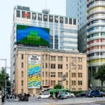
- South Jeolla chip plant plans trigger speculative rally in local stocksExpectations that Samsung Electronics and SK hynix will invest in massive chip plant projects in Gwangju and the surrounding South Jeolla Province have triggered a rally in various companies headquartered in the region. The rally has been fueled by expectations that the purported large-scale chip plants would spur demand for roads, transportation networks, housing and other public infrastructure needed to… Read more: South Jeolla chip plant plans trigger speculative rally in local stocks
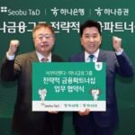
- Hana Financial Group partners with Seobu T&D on Seoul logistics complex projectHana Financial Group signed a memorandum of understanding (MOU) with real estate developer Seobu T&D to provide financing for an urban high-tech logistics complex in Seoul, the group said Sunday. The agreement establishes a partnership covering project finance, corporate finance and co-investment for Seobu T&D’s planned mixed-use development in Seoul’s Yangcheon District. The project will combine a smart logistics center… Read more: Hana Financial Group partners with Seobu T&D on Seoul logistics complex project

Latest Entertainment from Korea
- LE’V Steps Into the Light: “Spotlight Soul” Captures the Artistry, Growth, and Glow of a New Era in the 2026 Season’s Greetings CollectionPhoto Credits: CHROMOSOME LE’V Illuminates 2026 with “Spotlight Soul” LE’V enters 2026 with a statement that feels both cinematic and deeply personal. His Season’s Greetings “Spotlight Soul” concept photos reveal a striking evolution — one that merges emotional depth with artistic clarity. The project, released as a collector’s visual experience, celebrates not just another year but LE’V’s firm grasp on identity, craft,… Read more: LE’V Steps Into the Light: “Spotlight Soul” Captures the Artistry, Growth, and Glow of a New Era in the 2026 Season’s Greetings Collection
- KiiiKiii Leesol & Haum Illuminate SPUR x Dior Addict’s January 2026 Issue with Daring Light, Sensual Motion, and New Beauty CodesPhoto Credits: SPUR Dior Starship Entertainment A New Year, A New Iconic Pairing SPUR Magazine opens 2026 with a collaboration that feels both intimate and electric. The January 2026 Issue Pictorial Preview showcases KiiiKiii Leesol and Haum in a visual dialogue infused with Dior Addict’s luminous rebellion. Titled “Light Moves: The Addict State of Mind”, the spread captures the interplay of motion, reflection, and self-definition—a signal… Read more: KiiiKiii Leesol & Haum Illuminate SPUR x Dior Addict’s January 2026 Issue with Daring Light, Sensual Motion, and New Beauty Codes
- Breaking Boundaries: ifeye × KITTO Taiwan Redefine Visual Storytelling in the January 2026 Pictorial — A Fusion of Innovation & IdentityPhoto Credits: Hi-Hat Entertainment The Convergence of Vision and Identity The January 2026 Pictorial from ifeye × KITTO Taiwan marks a defining moment in East Asian creative media. Framed as both a celebration and an evolution, the collaboration bridges art direction, fashion narrative, and technological fluidity to capture a new generation’s pulse. More than a photoshoot, this issue acts as a visual manifesto—an exploration of… Read more: Breaking Boundaries: ifeye × KITTO Taiwan Redefine Visual Storytelling in the January 2026 Pictorial — A Fusion of Innovation & Identity
- Xiaoting in Full Bloom: Kep1er’s Shining Star Redefines Power, Grace, and Global Glamour in Wonderland China’s January 2026 Cover StoryPhoto Credits: KLAP ENTERTAINMENT Kep1er’s Xiaoting Captures the Moment Kep1er’s Shen Xiaoting steps into 2026 as a muse of modern elegance, fronting the January 2026 Wonderland China cover with an aura that’s both futuristic and fiercely grounded. As one of the brightest stars of her generation, Xiaoting embodies the balance between aspiration and artistry that defines global pop’s next chapter. “Confidence is not just… Read more: Xiaoting in Full Bloom: Kep1er’s Shining Star Redefines Power, Grace, and Global Glamour in Wonderland China’s January 2026 Cover Story
- BTS’s V Radiates Timeless Charisma in GQ Korea x Cartier’s February 2026 Cover: A Monument to Modern Elegance and Emotional PrecisionPhoto Credits: GQ Korea – Cartier – BigHit Music. – BTS V x Cartier: The Sound of Stillness and Strength For GQ Korea’s February 2026 issue, the cover unfolds like a cinematic confession. BTS’s V (Kim Taehyung)—known for his magnetic duality of mystery and warmth—joins forces with Cartier, the house synonymous with precision, artistry, and legacy. Together, they create a visual symphony that celebrates… Read more: BTS’s V Radiates Timeless Charisma in GQ Korea x Cartier’s February 2026 Cover: A Monument to Modern Elegance and Emotional Precision


Learn People & History of Korea
- The Evolution of Busan: A Historical Journey Through South Korea’s Second Largest Metropolitan CityAncient Beginnings: The Founding of Busan Busan, known as the second largest metropolitan city in South Korea, has a rich history that dates back to ancient times. The earliest recorded existence of Busan can be traced to the Goryeo Dynasty, where it was referenced as a vital coastal settlement. Its strategic location along the southeastern coast of the Korean Peninsula… Read more: The Evolution of Busan: A Historical Journey Through South Korea’s Second Largest Metropolitan City
- The Evolution of Pyongyang: A Journey Through History, Economy, and Political DynamicsIntroduction to Pyongyang Pyongyang, the capital city of North Korea, serves as a prominent symbol of the nation’s history and culture. Geographically located on the banks of the Taedong River, in the southwest part of the country, Pyongyang is situated within a strategic area that has historically facilitated trade and cultural exchange. The city’s origins can be traced back to… Read more: The Evolution of Pyongyang: A Journey Through History, Economy, and Political Dynamics
- The Evolution of Seoul: From Ancient Korea to Modern Metropolis and BeyondAncient Beginnings: The Founding of Seoul The city of Seoul, known today as the vibrant capital of South Korea, has ancient roots that trace back to the Three Kingdoms period of Korea, specifically the kingdoms of Baekje and Silla. Evidence suggests that Seoul was originally established as a settlement given its strategic geographical advantages. Nestled within the Han River basin,… Read more: The Evolution of Seoul: From Ancient Korea to Modern Metropolis and Beyond
- Exploring Korean Traditional Games in Squid Game: From Season 2 to Upcoming Season 3Introduction to Korean Traditional Games Korean traditional games have long been an integral part of the country’s cultural landscape, offering more than mere entertainment. These games, which range from simple children’s pastimes to complex community activities, hold significant cultural significance and often serve as a means of preserving history and promoting social interaction. Rooted in centuries of tradition, these games… Read more: Exploring Korean Traditional Games in Squid Game: From Season 2 to Upcoming Season 3
- Unveiling the Past and Present of Saju: The Art of Korean Fortune TellingIntroduction to Saju Saju, a traditional Korean fortune-telling practice, is an intricate art that seeks to interpret an individual’s fate based on their birth date and time. The term “Saju” translates to “four pillars” in English, referring to the four critical components derived from these time markers: year, month, day, and hour. This method holds significant cultural value within South… Read more: Unveiling the Past and Present of Saju: The Art of Korean Fortune Telling