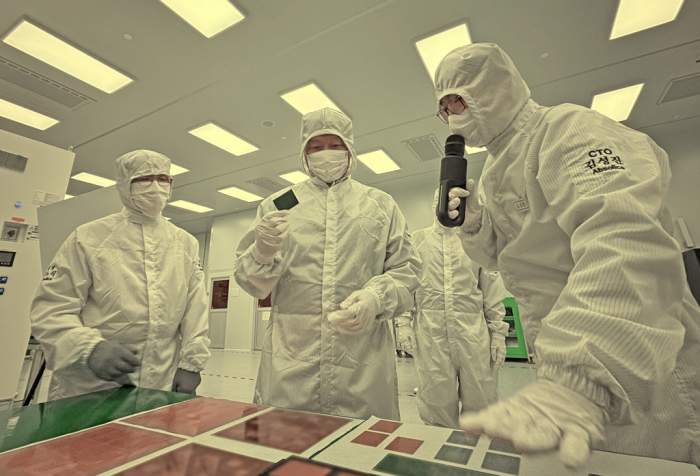
Absolics Inc., the US glass substrate affiliate of South Korean chemical materials company SKC Ltd., has been selected to receive up to $100 million in research and development grants from the Department of Commerce.
According to the Commerce Department, Absolics is one of three recipients of $300 million investment funds set up under the National Advanced Packaging Manufacturing Program (NAPMP), part of the CHIPS for America project designed to boost the US semiconductor industry.
The other two recipients are Applied Materials Inc. in California and Arizona State University.
According to the department, each recipient will receive up to $100 million in R&D investment.
Absolics has already received $75 million in production subsidies under the CHIPS Act. With the latest R&D grant, the company has been further recognized for its advanced glass substrate technology.
“The research investments represent novel efforts in advanced substrates… This combined effort will help ensure US manufacturers stay competitive and continue to drive technological innovation, giving companies a stronger edge in global competition,” the department said in a statement.

ADVANCED CHIP PACKAGING: A GAME CHANGER
Chip packaging is the final stage of semiconductor device fabrication to protect chip materials and connect the chips to a circuit board. Advanced packaging technology has become more important as chip capacity expansion through process technology is nearing its upper limit.
SKC, a unit of Korea’s second-largest conglomerate SK Group, acquired US glass substrate maker Absolics for $240 million In 2021.
Absolics is currently building a plant in Covington, Georgia to produce next-generation glass substrate – a thin layer of glass on which memory chips are mounted to create the brain of a computing system.
The company aims to begin mass production by the end of 2025.
The Covington plant is the world’s first mass-production facility for glass substrates, with an annual capacity of 12,000 square meters. Absolics plans to build a second plant with an annual capacity exceeding 72,000 square meters.
With a thickness that is only a fourth that of a conventional printed circuit board (PCB), a glass substrate makes it easier to miniaturize chip packaging, significantly increasing the performance and energy efficiency of chipsets.

IN PARTNERSHIP WITH 30 US PARTNERS
Absolics said it aims to revolutionize glass core substrate panel manufacturing by developing cutting-edge capabilities in partnership with over 30 partners including academic institutions, large and small businesses and non-profit entities.
As part of efforts to enhance its presence in the US substrate market, SKC acquired a 12% stake in Chipletz, a US fabless substrate startup that specializes in semiconductor packaging. It didn’t disclose its investment amount.
The US government said the National Advanced Packaging Manufacturing Program set aggressive technical targets for the substrates that all three entities are expected to meet or exceed.
“Advanced packaging is essential to the development of the advanced semiconductors that are the drivers of emerging technology like artificial intelligence,” said Under Secretary of Commerce for Standards and Technology and National Institute of Standards and Technology Director Laurie E. Locascio.
By Jeong-Soo Hwang
hjs@hankyung.com
In-Soo Nam edited this article.


