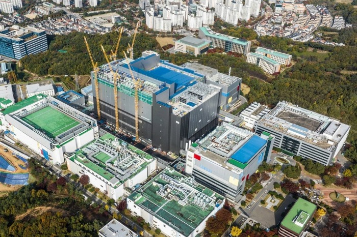
Samsung Electronics Co. is pinning high hopes on its new research and development complex, which will cost the company a total of 20 trillion won ($14.4 billion), to regain ground in the chip market after losing ground to its smaller cross-town rival SK Hynix Inc. in a high-bandwidth memory war.
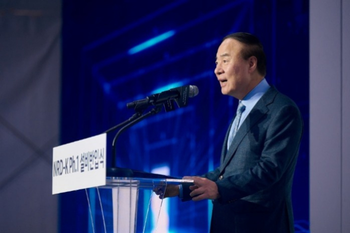
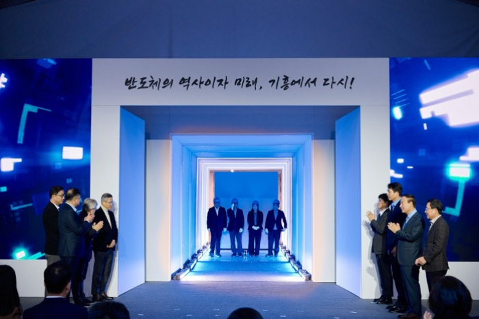
“NRD-K will bolster our development speed, enabling the company to create a virtuous cycle to accelerate fundamental research on next-generation technology and mass production,” Jun Young-hyun, vice chairman and head of the Device Solutions Division at Samsung Electronics, said at a ceremony held on Monday to celebrate the beginning of equipment installation at Samsung’s new R&D complex, dubbed NRD-K.
“We will lay the foundation for a new leap forward in Giheung, where Samsung Electronics’ 50-year history of semiconductors began, and create a new future for the next 100 years,” Jun added.
The company will spend a total of 20 trillion won on the complex, which is expected to play a critical role in developing and producing next-generation semiconductors such as artificial intelligence chips, by 2030.
The Korean chip giant, which is the world’s largest memory chipmaker, is currently lagging behind the runner-up SK Hynix in an AI chip race after it has not yet passed the world’s No. 1 AI chip maker Nvidia Inc.’s quality test for HBM chips.
SK Hynix is the world’s leading HBM chip supplier with a market share of 53%, followed by Samsung Electronics with 35%.

With the new R&D center, Samsung Electronics will strive to catch up to SK Hynix in the HBM chip market, which is forecast to grow to $33 billion in 2027 from $4 billion in 2023, according to Morgan Stanley.
The R&D complex, which will be built on a land of 109,000 square meters in Samsung Electronics’ Giheung campus, will house chip development and production R&D facilities – systems foundry – under one roof to accelerate next-generation chip development.
It will begin the operation of an R&D-dedicated line in mid-2025.
THE CENTER OF NEXT-GEN CHIP R&D AND PRODUCTION
NRD-K will be equipped with advanced equipment and infrastructure, including high NA extreme ultra-violet (EUV) lithography and new material deposition equipment, to develop future-leading memory chips such as 3D dynamic random access memory (DRAM) and V-NAND with more than 1,000 layers.
Samsung Electronics will also set up a wafer bonding infrastructure for wafer-to-wafer bonding in the complex.
The state-of-the-art R&D complex is also expected to help expand the Korean semiconductor industry’s raw materials, parts and equipment R&D ecosystem considering Giheung is home to many related companies from around the world, including Korea.

“At a time when the importance of win-win partnerships is greater than ever, Applied Materials is committed to accelerating innovation velocity through deep collaboration with Samsung Electronics, working together to drive a new wave of growth for the semiconductor industry,” said Park Gwang-sun, head of Applied Materials Korea.
Samsung Electronics Executive Chairman Jay Y. Lee urged employees to make a turning point for innovation to take another leap amid ongoing local and international crises during his visit to the construction site of NRD-K in October last year.
Samsung’s semiconductor business took off from the Giheung campus in 1983 when the Korean company threw down the gauntlet to bigger Japanese chip giants at that time.
The place was the birthplace of the world’s first 64-megabyte (Mb) DRAM chips in 1992.
Samsung’s chip business head Jun vowed to take drastic steps to improve profitability and regain memory leadership after flagging the company’s weaker-than-expected third-quarter earnings in early October.
By Eui-Myung Park
uimyung@hankyung.com
Sookyung Seo edited this article.


