
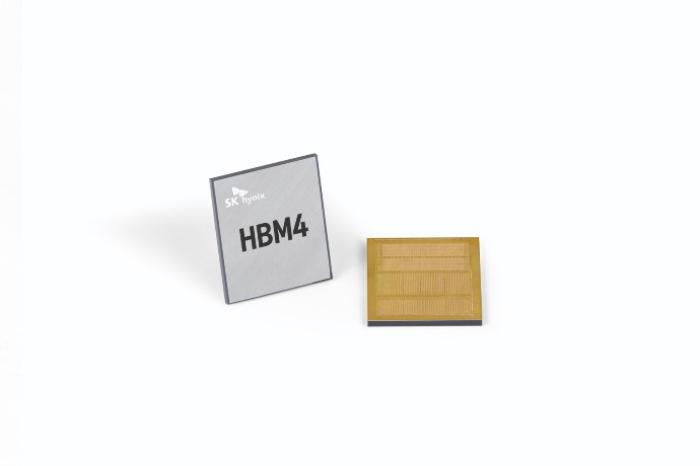
South Korean memory chip giant SK Hynix Inc. has begun delivering samples of the world’s most advanced, next-generation high bandwidth memory chip, the 12-layer HBM4, to its key customers ahead of its original schedule, further widening its lead over rivals.
The HBM pioneer, a core supplier to artificial intelligence chip leader Nvidia Corp. and other AI chipmakers, announced on Wednesday that it had delivered the first HBM4 samples to its customers for quality evaluation six months earlier than its original timeline, which was early 2026.
SK Hynix said it plans to get ready for mass production of the 12-layer HBM4 within the second half of this year for the immediate start of its supply.
The faster-than-planned sample supplying comes in response to mounting pressure from its customers asking for faster, more efficient memory for next-generation AI applications, especially Nvidia, amid an intensifying AI race.
The sixth-generation high-performance memory chip is expected to be fitted in Nvidia’s next-generation graphics architecture Vera Rubin, the successor of the Blackwell AI chip.
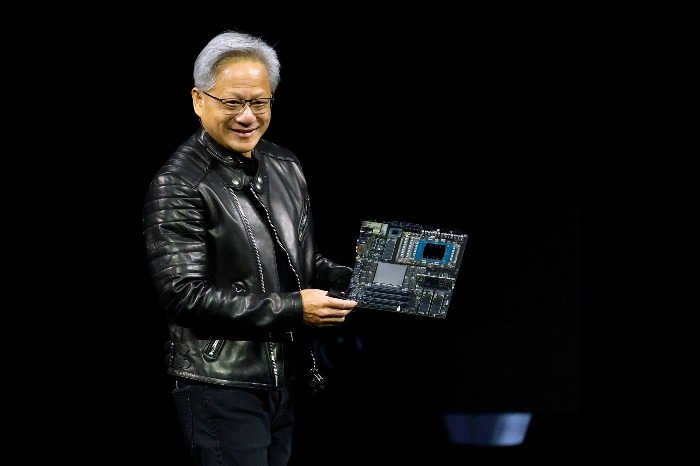
On Tuesday, Huang said at the Nvidia GPU Technology Conference (GTC) 2025 – dubbed the “Super Bowl of AI” – that Blackwell Ultra is slated for the second half of 2025, while the Rubin AI chip is expected to launch in late 2026.
This is also the first HBM chip developed in collaboration between SK Hynix and global top foundry player Taiwan Semiconductor Manufacturing Co. (TSMC).
It said it would adopt TSMC’s advanced logic process for its HBM4’s base die, which is placed at the bottom of an HBM connected to a graphics processing unit and acts as its brain.
MOST ADVANCED HBM
SK Hynix’s latest innovation boasts the industry’s best capacity and speed, which are essential for AI processors that handle vast amounts of data, said the company.
Its 12-layer HBM4 is the industry’s first HBM capable of processing more than 2 terabytes (TB) of data per second. This means data equivalent to more than 400 full-HD movies (5GB each) can be processed in a second, more than 60% faster than the previous generation, the HBM3E, explained the company.
The Korean chipmaker also adopted the advanced MR-MUF process, which helps prevent chip warpage and maximizes product stability by improving heat dissipation, to achieve a capacity of 36GB, the highest among 12-layer HBM products.
SK Hynix has long been a leader in HBM development, holding an estimated 50% market share in the global HBM chip market.
It succeeded in mass-producing the 8- and 12-layer HBM3E in 2024, becoming the world’s first to supply the 12-high HBM3E to Nvidia.
AT GTC 2025
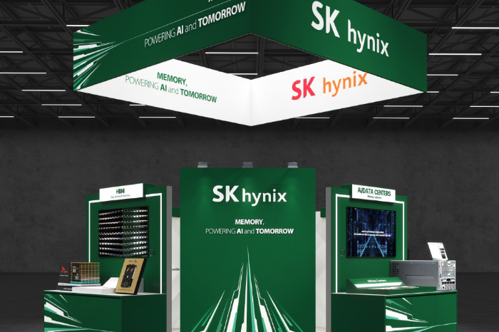
The Korean chipmaker will showcase its HBM and other memory products for AI data centers, as well as on-device and memory solutions for automotive applications at GTC 2025, a global AI conference taking place on March 17-21 in San Jose, CA.
It will present the 12-high HBM3E and SOCAMM2, or small outline compression attached memory module, for AI servers, as well as a model of the 12-high HBM4.

HBM technology, which stacks multiple dynamic random access memory (DRAM) chips vertically to accelerate data transfer speeds, has become a cornerstone of the AI revolution.
Nvidia, the dominant force in AI processing, has leaned heavily on HBM technology to enhance its high-end GPUs, which power large-scale AI models such as OpenAI’s ChatGPT.
Rivals Samsung Electronics Co. and Micron Technology Inc. are also working on next-generation HBM solutions, aiming to capture a share of the growing AI infrastructure market.
Especially, SK Hynix’s cross-town rival Samsung recently outlined aggressive expansion plans for its HBM capacity but it is behind SK Hynix in terms of both technology prowess and schedule.
By Chae-Yeon Kim
why29@hankyung.com
Sookyung Seo edited this article.