
SK Hynix Inc., the world’s top DRAM memory chipmaker, aims to redefine the competitive landscape in artificial intelligence memory chips with plans to introduce vertically stacked 3D HBM from its fifth-generation high-bandwidth memory (HBM5).
The South Korean chipmaker is actively researching the implementation of three-dimensional HBM, a transformative architecture in which DRAM chips are stacked on top of the graphics processing unit (GPU), rather than placed alongside it, an SK Hynix executive said at a tech seminar on Thursday.
“Stacking DRAM vertically on the GPU can be a game-changer,” Lee Kang-wook, vice president and head of SK Hynix’s package development division, said during his keynote speech at the Institute of Electronics and Information Engineers’ annual conference.
He said the architectural leap would significantly reduce data transmission latency while improving bandwidth and power efficiency, key metrics in the performance-hungry AI industry.
The executive unveiled the company’s HBM roadmap that would see 3D HBM rolled out, beginning with HBM5 – a product still several generations ahead.
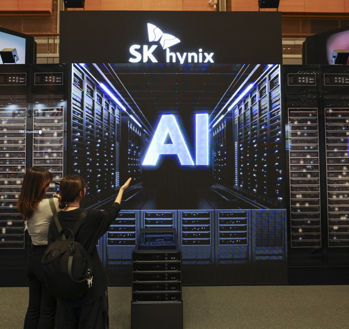
SK Hynix currently leads the industry in HBM development.
Its HBM3E chips are in mass production, with HBM4 expected to launch later this year, followed by HBM4E in 2026.
The potential introduction of 3D stacking in HBM5 marks a long-term strategy to secure technological dominance in memory chips powering generative AI models, he said.
RED-HOT AI CHIP MARKET
The race for 3D chip packaging tech gets even fiercer as shrinking chips becomes increasingly challenging.
SK Hynix’s crosstown rival, Samsung Electronics Co., is also working on 3D chip packaging technology as it struggles to catch up to foundry, or contract chipmaking, leader Taiwan Semiconductor Manufacturing Company (TSMC).
SAINT, or Samsung Advanced Interconnection Technology, aims to integrate memory and processors required of high-performance chips, including AI chips, in much smaller sizes.
Packaging, one of the final steps in semiconductor manufacturing, places chips in a protective case to prevent corrosion and provides an interface to combine and connect already-made chips.
Leading chipmakers such as TSMC, Samsung and Intel Corp. are fiercely competing for advanced packaging, which integrates different semiconductors or vertically interconnects multiple chips. Advanced packaging allows multiple devices to be merged and packaged as a single electronic device.
Packaging technology can enhance semiconductor performance without having to shrink the nanometer scale through ultra-fine processing, which is technologically challenging and requires more time.
HYBRID BONDING
Lee, the SK Hynix executive, said the company also plans to introduce hybrid bonding technology from the HBM4E generation, which will feature 20-layer stacked DRAM chips.
Up to the 16-layer sixth-generation HBM, or HBM4, the company uses MR-MUF technology, which involves connecting DRAM layers with micro bumps and filling the gaps with a liquid material.
Starting from 20-layer stacking, however, hybrid bonding is essential, he said.
Hybrid bonding connects semiconductor layers directly through copper-to-copper contact, eliminating the need for micro-bumps and allowing for thinner chips with improved thermal dissipation.
The company expects the new bonding method to offer further advantages in performance and energy efficiency.
Beyond hardware innovation, SK Hynix is actively working to secure customers for its advanced 2-nanometre process nodes.
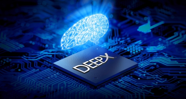
One such customer is DeepX, a domestic AI chip startup, which recently signed on as one of its 2 nm clients – a milestone that underscores SK Hynix’s growing role in Korea’s AI semiconductor ecosystem.
DeepX specializes in AI semiconductors embedded in applications such as physical security, robotics, home appliances, smart mobility and smart cameras.
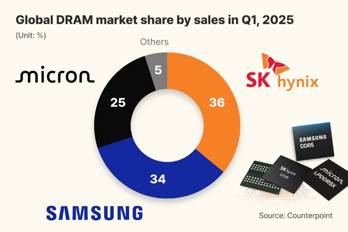
The move comes amid intensifying global competition in the AI chip supply chain, with industry giants such as Nvidia Inc., TSMC, Samsung and Micron Technology Inc. vying to secure performance and scale advantages in memory technologies critical to large language models and high-performance computing.
By Jeong-Soo Hwang
hjs@hankyung.com
In-Soo Nam edited this article.