ASML Holding NV, the Dutch tech giant and sole producer of extreme ultraviolet (EUV) lithography machines in the world, is expected to discuss ways to strengthen chip technology collaboration with Samsung Electronics Co. and SK Hynix Inc., the world’s two largest memory chipmakers, during CEO Christophe Fouquet’s first visit to Seoul this week.
Fouquet, who took office as ASML’s president and chief executive in April last year, is making his first trip to South Korea this week to attend the opening of the company’s new headquarters in Dongtan, south of Seoul, on Wednesday.
The new facility serves as ASML’s strategic base in the country, home to the world’s top two memory chip producers.
During the visit, Fouquet is expected to meet Samsung Electronics Chairman Lee Jae-yong and SK Group Chairman Chey Tae-won to discuss next-generation chipmaking technologies and cooperation in advanced manufacturing.

DEEPENING COLLABORATION IN HIGH-NA EUV
Industry officials said ASML and Samsung are expected to expand collaboration on high numerical aperture (NA) EUV lithography, the next-generation exposure technology that enables ultra-fine patterning required for 2-nanometer and smaller process nodes.
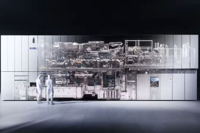
Samsung plans to introduce the technology in two phases, taking delivery of its first high NA EUV scanner, the Twinscan EXE:5200B, later this year, followed by a second unit in the first half of 2026.
The company already operates a research-use high NA EUV tool at its Hwaseong campus, but the upcoming machines will mark its first purchases intended for mass production.
The high NA EUV system, developed by ASML, features a numerical aperture of 0.55, up from 0.33 in current-generation EUV tools, enabling 1.7 times finer circuit etching.
This precision allows chipmakers to produce ultra-dense circuitry required for next-generation logic and memory chips, including 2-nm foundry products and vertical channel transistor (VCT) DRAMs.

Each unit costs roughly 550 billion won ($375.4 million), making it the most expensive piece of equipment in semiconductor manufacturing, underscoring the scale of Samsung’s investment to maintain a technological edge over competitors such as Taiwan Semiconductor Manufacturing Co. (TSMC) and Intel Corp. in foundry.
SK Hynix became the first in the world to install a high NA EUV machine for mass production at its Icheon M16 fab in September, targeting VCT DRAM production.
Following the ASML CEO’s Seoul visit, the Dutch company and Samsung are also expected to accelerate their plan to build a joint research and development center in South Korea, a 700 million euros ($810 million) project designed to jointly advance chip technology and EUV process technology.
The site is in the final location selection, with construction expected to begin soon.
FOUNDATION FOR AI-ERA SEMICONDUCTORS
Samsung was the first in the industry to apply conventional EUV lithography to its 7-nm foundry line in 2018 and later to DRAM production in 2020.

The new high NA generation represents the next leap, enabling the ultra-precise patterning required for advanced chips that power artificial intelligence and data-intensive applications.
Sources said Samsung plans to deploy the new machines at its 2-nm foundry lines, which already produce Exynos 2600 application processors.
The Korean chipmaker also plans to manufacture and supply Tesla Inc.’s next-generation AI chips at the 2-nm lines using the latest EUV equipment.
Analysts said the move signals that Samsung, after a period of cautious capital spending, is shifting back into aggressive investment mode to close the gap with competitors, including dominant foundry player TSMC.
Samsung has recently narrowed the performance divide with SK Hynix in next-generation high-bandwidth memory (HBM), selling off its sixth-generation HBM4E chips to key customers next year after winning long-awaited validation from Nvidia Corp. for the fifth-generation 12-layer HBM3E product in September.